EMSI Conference brings forth the new trends
Paves way for greater research in Nano science

Inauguration of National Conference on Electron Microscopy and Allied Fields at Bundelkhan University, Jhansi

Scientific Exhibition at the Conference
The National Conference of Electron Microscope Society of India (EMSI – 2009) was held at Bundelkhand University in Jhansi from January 17-19, 2009. This annual conference promoted interdisciplinary research, bridging various scientific and technical disciplines. The conference brought various scientists from across the country to work in different disciplines to discuss the various aspects of microscopy.
Dr Peter Koshy, outgoing president of EMSI, mentioned that, “Electron Miscroscopy has paved way to the birth nanotechnology, but this has not really got its due importance in the country for various reasons. Thanks to major push in nanotechnology by the government and private organizations, this field is now looked forward.”
The electron microscope needs no introduction. It has been hailed as one of the most important inventions of the 20th century. Since it was first unveiled, the electron microscope has undergone many technical improvements and seen the incorporation of new designs, among them the scanning tunneling electron microscope. But nonetheless, the pioneering attempt of Ernst Ruska was rewarded with one half of the 1986 Nobel Prize in Physics for his fundamental work in electron optics and for the design of the first electron microscope. The other half went jointly to Dr Gerd Binnig and Dr Heinrich Rohrer for their design of the scanning tunneling microscope. Today almost no branch of science can do without electron microscope, which has been the tool to reveal many of nature’s mysteries.
The conference discussed advances in the electron microscopy techniques as also the understanding of new and exotic materials and their consequent applications of relevance to the society. More importantly, the new nanoscale analytical techniques have made it possible to understand and also help create matter on a nanoscale and thus have ushered in an era of what is now popularly called nano science and nanotechnology.
Explaining about the importance newly appointed president of EMSI R P Tandon says, “Today our country is being recognized for its large pool of excellent human resources in science and technology and it is high time they are brought to the lime light. In view of encouraging our scientists, academicians, and young researchers for the future, this is the purpose of the conference.”
EMSI found one of its missions to identify the scientific brilliance in the country, recognize their scientific contributions and honour them with different prestigious awards during the annual meeting. Dr Srikumar Banerjee, director of Baba Atomic Research Centre, Mumbai was presented with Lifetime Achievement Award for 2008-09 while Dr PD Gupta of CCMB was given the same award in Biological Sciences category. For the first time the Society has instituted Fellow of EMSI and has given this honour to 10 prominent people: Prof K Chattopadhyay, Dr MS Rao, Dr Fazil Marickar, Prof RP Tandon, Dr G K Dey, Dr Sudip Dey, Dr Sabu Thomas, Dr Indradev Samajdar, Dr P Prabhakar Rao and Dr Prakash Kumar.
Apart from the conference, there was a scientific exhibition with various corporate players displaying their newest products and technologies. Major players participated in this much awaited exhibition: Icon Analytical, Gatan, Jeol, Blue Star, Carl Zeiss, Forevision Instruments, Oxford Instruments, Camscan, Mars Scientific & Bruker Miscroanalysis, Tinsley-Wayne Kerr, Sree Analytical, Labindia Instruments, Ants Ceramics, Metrex and Advance Scientific & Tescan.
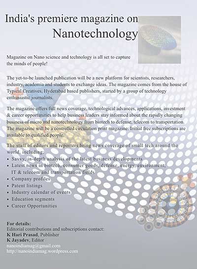
Nano India magazine took this opportunity to meet and inform about the impending launch of the magazine. Flyers were distributed to all the participants of the conference generating curiosity to know about the magazine.
Filed under: events, Sciences, conference, electron microscope, electron optics, EMSI, events, nanotechnology, scanning tunneling microscope


Recent Comments